
Groups
Nanoparticles and Nanodispersions
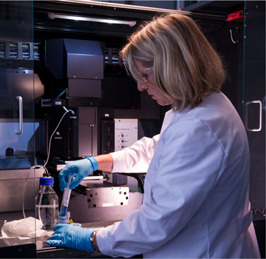
 Nanoparticle Process Technology (NPPT) was a newly founded division (chair) in 2003 as part of the Faculty of Engineering, Department of Mechanical Engineering and Process Engineering at the University of Duisburg-Essen (UDE). NPPT, headed by Professor Markus Winterer, covers the synthesis of and structuring with nanoparticles using advanced methods of chemical reaction engineering, measurement technology, characterization, modeling and simulation in teaching and research. The research topic of the Winterer group within the framework of the Virtual Institute ‘Printed Electronics based on Inorganic Nanomaterials: From atoms to functional devices and circuits’ is to master the complexity involved in printing of colloidal dispersions containing small semiconductor nanoparticles, especially using ink-jet technology. The tasks are twofold: firstly, preparation of semiconducting nanoparticles with suitable sizes, shapes, morphology, carrier concentration and doping (n- or p-type) level and secondly, the preparation of printable nanoinks with proper rheology and a minimum of stabilizing additives.
Printed Oxide Electronics using Electrolytic Insulators
The group of Printed Electronics at Institute of Nanotechnology (INT), Karlsruhe Institute of Technology (KIT) is specialized in oxide field-effect transistor, ink-jet printing and novel printable gate insulators, such as composite solid polymer electrolytes. the role of the group within the Virtual Institute is to provide high performance (high mobility and transconductance) field-effect transistors and logic circuits on rigid, as well as on flexible substrates, that are preferably all-printed, all-room temperature processed, can operate at low operating voltages, and at moderate to high operation frequencies. The group also focus on active participation with partners in evaluating electrical and mechanical reliability of printed devices.

Printed Oxide Electronics using Organic/Inorganic or Hybrid Dielectrics
The Electronic Materials group at Technical University Darmstadt (TUD) is well-established in the field of organic semiconducting devices in particular in organic field-effect transistors. However, presently the von Seggern group is also concentrating in the field of inorganic semiconductor based field-effect transistors. Here the focus can be seen on presursor-based metal oxides, such as zinc oxide (ZnO) and indium zinc oxide (IZO) as well as ZnO devices made from nanoparticulate dispersions. Within the Virtual Institute (VI) the TUD competence will be utilized in order to produce and characterize top-gated field-effect transistors with organic and inorganic dielectrics. Typically, the organic dielectrics are easily solution processable, thus will be particularly suitable for printing. Even though one aim of the VI is the preparation of all-printed devices, evaporated dielectrics will also be examined.

Mechanical Reliability (Tensile & Bending Tests) of Printed Devices
The group at IAM-WBM, Karlsruhe Institute of Technology (KIT) is well established in the area of reliability studies using state-of-the-art equipment such as in-situ SEM and synchrotron radiation to study the mechanical, thermal, and electric fatigue of structural and functional materials. Printed electronics on flexible substrates have to survive large strains over their entire lifetime. Therefore, static and cyclic mechanical tests (tensile and bending tests) of such circuits and systems are mandatory to predict their reliability, lifetime and to identify the predominant mechanisms of failure. This allows for the development of lifetime models for the devices produced in the VI, and will also guide to a failure tolerant design which includes feedback to the design groups. From a fundamental materials side, the character of interfaces that results in maximal adhesion will be investigated and the influence of elastic strain on semiconductors in the device will be addressed as a potential damage mechanism, but also as a possible pathway to tune semiconductor properties.

Mechanical Reliability (Microstructural Relation to Electrical Performance) of Printed Devices
The Laboratory for Nanometallurgy at ETH Zurich is specialized on complex characterization of heterogeneous systems (metallic, semiconducting, ceramics, composites, etc) produced in the form of thin films, coatings, and patterned nanoparticles assemblies. Microstructural and phase analyses of these systems are accompanied by Raman and RDS spectroscopic studies. Moreover, the analyses are iteratively related to the mechanical and electrical performances of the systems by different in-situ testing techniques.
Modeling, Robust Circuit Design and Analysis of Printed Electronics
The Chair of Dependable Nano Computing (CDNC) at Karlsruhe Institute of Technology (KIT) is part of the Department of Computer Science (ITEC). The main research area of the chair revolves around dependable computing at nanoscale (test and reliability) and emerging nanotechnologies for computing. The responsibility of the chair within the Virtual Institute (VI) is first to perform an electrical characterization of inorganic transistors (IV, capacitances) in order to develop an empirical model. Through collaboration with other partners of the VI, working on physical parametric equations for compact models, by fitting parameters, we plan for integration and reformulation of this into a SPICE compatible model, which will serve as an input to the design system. Later, the models will be used to design basic standard cells, such as INV, NAND, NOR, 2X, 4X, Ring oscillators using organic printed transistors. Another important consideration is the technology assessment for suitable/possible applications of printed electronics.