Vision & Structure
Aim
Our aim is to launch a comprehensive research effort to develop the science and technology for the reliable production scheme of commercially relevant inorganic oxide based printed electronics.
Background
Printed electronics based on inorganic materials have a distinct advantage because of their high-carrier mobility and the environmental stability of inorganic semiconductors. For example, oxides show clearly superior transport properties compared to the organic semiconductors.
Nevertheless, inorganic semiconductors (specifically oxides) have not previously been used for printed electronics, primarily because solution processing of inorganic materials is difficult and high performances are only obtained at temperatures above the glass transition of commonly used, inexpensive flexible substrates, such as polymers, papers etc.
Objectives
Our primary objective is to demonstrate fully room-temperature processed high-performance oxide electronics that are printed on low-temperature endurable and flexible substrates. We also intend to demonstrate improved reliability (electrical, thermal, mechanical) for printed inorganic (oxide) electronics and to develop benchmark performance parameters with multi-scale modeling at the device and the circuit level.
Structure
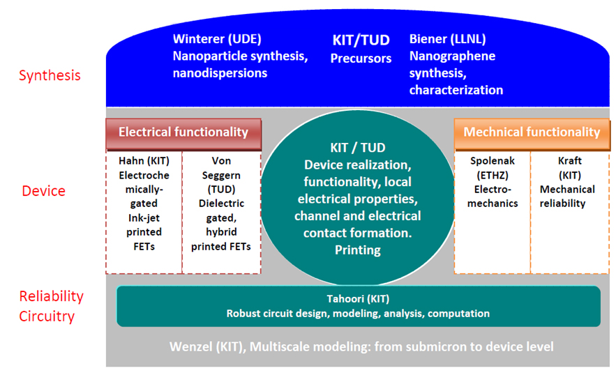
As a Helmholtz Virtual Institute, we are coordinated through the Karlsruhe Institute of Nanotechnology (KIT) and combine our efforts through four additional university partners: TU Darmstadt (TUD), University Duisburg-Essen (UDE), ETH Zurich (ETHZ), and the Lawrence Livermore National Laboratory (LLNL).
Cooperative Activities
The individual activities and success of the undertaking are truly dependent and interlinked with each other. The high quality raw materials are supplied by the UDE (for example, nontrivial p-type oxide semiconductors) and LLNL (carbon based conducting and semiconducting materials) scientists. KIT (INT) and TUD researchers cooperate on device fabrication and characterization (integrated CMOS logics, ring oscillators). And mechanical reliability of the devices is tested at KIT (IAM) and is supported by ETHZ with their strong expertise in electromechanics.
Additionally, multi-scale modeling of printed FETs will be performed at KIT (INT) based on drift-diffusion simulation of realistic printed semiconductor layer morphologies, which may later be used to simulate full device and circuits. The circuit simulation group at KIT (ITEC) focuses their efforts on create a cell library in general for electrolyte-gated oxide electronics, which may later be used to simulate rather complex circuits consisting of individual EG FET building blocks.

